- 您现在的位置:买卖IC网 > Sheet目录317 > CAT24C08TDI-GT3 (ON Semiconductor)8KB I2C SER EEPROM TSOT 23
�� �
�
�CAT24C01,� CAT24C02,� CAT24C04,� CAT24C08,� CAT24C16�
�V� CC�
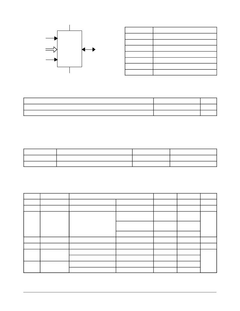
�Table� 1.� PIN� FUNCTION�
�Pin� Name� ?�
�Function�
�SCL�
�A0,� A1,� A2�
�SDA�
�Device� Address� Input�
�Serial� Data� Input/Output�
�A� 2� ,� A� 1� ,� A� 0�
�CAT24Cxx�
�SDA�
�SCL�
�Serial� Clock� Input�
�WP�
�Write� Protect� Input�
�WP�
�V� CC�
�V� SS�
�NC�
�Power� Supply�
�Ground�
�No� Connect�
�V� SS�
�Figure� 1.� Functional� Symbol�
�Table� 2.� ABSOLUTE� MAXIMUM� RATINGS�
�?The� exposed� pad� for� the� TDFN/UDFN� packages� can� be� left� floating�
�or� connected� to� Ground.�
�Parameters�
�Storage� Temperature�
�Voltage� on� any� pin� with� respect� to� Ground� (Note� 1)�
�Ratings�
�?� 65� to� +150�
�?� 0.5� to� +6.5�
�Units�
�°� C�
�V�
�Stresses� exceeding� Maximum� Ratings� may� damage� the� device.� Maximum� Ratings� are� stress� ratings� only.� Functional� operation� above� the�
�Recommended� Operating� Conditions� is� not� implied.� Extended� exposure� to� stresses� above� the� Recommended� Operating� Conditions� may� affect�
�device� reliability.�
�1.� During� input� transitions,� voltage� undershoot� on� any� pin� should� not� exceed� ?� 1� V� for� more� than� 20� ns.� Voltage� overshoot� on� pins� A� 0� ,� A� 1� ,� A� 2�
�and� WP� should� not� exceed� V� CC� +� 1� V� for� more� than� 20� ns,� while� voltage� on� the� I� 2� C� bus� pins,� SCL� and� SDA,� should� not� exceed� the� absolute�
�maximum� ratings,� irrespective� of� V� CC� .�
�Table� 3.� RELIABILITY� CHARACTERISTICS� (Note� 2)�
�Symbol�
�N� END� (Note� 3)�
�T� DR�
�Endurance�
�Data� Retention�
�Parameter�
�Min�
�1,000,000�
�100�
�Units�
�Program� /� Erase� Cycles�
�Years�
�2.� These� parameters� are� tested� initially� and� after� a� design� or� process� change� that� affects� the� parameter� according� to� appropriate� AEC� ?� Q100�
�and� JEDEC� test� methods.�
�3.� Page� Mode,� V� CC� =� 5� V,� 25� °� C.�
�Table� 4.� D.C.� OPERATING� CHARACTERISTICS�
�(V� CC� =� 1.8� V� to� 5.5� V,� T� A� =� ?� 40� °� C to +125� °� C and V� CC� = 1.7 V to 5.5 V, T� A� =� ?� 40� °� C to +85� °� C, unless otherwise� specified.)�
�Symbol�
�I� CCR�
�I� CCW�
�Parameter�
�Read� Current�
�Write� Current�
�Test� Conditions�
�Read,� f� SCL� =� 400� kHz�
�Write,� f� SCL� =� 400� kHz�
�Min�
�Max�
�1�
�2�
�Units�
�mA�
�mA�
�I� SB�
�Standby� Current�
�All� I/O� Pins� at� GND� or� V� CC�
�T� A� =� ?� 40� °� C� to� +85� °� C�
�V� CC� ≤� 3.3� V�
�1�
�m� A�
�T� A� =� ?� 40� °� C� to� +85� °� C�
�V� CC� >� 3.3� V�
�T� A� =� ?� 40� °� C� to� +125� °� C�
�3�
�5�
�I� L�
�V� IL�
�I/O� Pin� Leakage�
�Input� Low� Voltage�
�Pin� at� GND� or� V� CC�
�?� 0.5�
�2�
�0.3� x� V� CC�
�m� A�
�V�
�V� IH�
�Input� High� Voltage�
�A� 0� ,� A� 1� ,� A� 2� and� WP�
�0.7� x� V� CC�
�V� CC� +� 0.5�
�V�
�SCL� and� SDA�
�0.7� x� V� CC�
�5.5�
�V� OL�
�Output� Low�
�Voltage�
�V� CC� >� 2.5� V,� I� OL� =� 3� mA�
�V� CC� <� 2.5� V,� I� OL� =� 1� mA�
�0.4�
�0.2�
�http://onsemi.com�
�2�
�发布紧急采购,3分钟左右您将得到回复。
相关PDF资料
CAT24C128HU4IGT3
IC EEPROM 128KB I2C SRL 8UDFN
CAT24C164YI-G
IC EEPROM SERIAL 16KB I2C 8TSSOP
CAT24C208WI-GT3
IC EEPROM SER 8KB 400KHZ 8SOIC
CAT24C21LI
IC EEPROM SERIAL 1KB DUAL 8PDIP
CAT24C256XI-T2
IC EEPROM 256KBIT 400KHZ 8SOIC
CAT24C32HU3I-GT3
IC EEPROM 32KB I2C SERIAL 8UDFN
CAT24C32TSI-T3
IC EEPROM SRL 32KB I2C 5TSOP
CAT24C512HU5IGT3
IC EEPROM SRL 512KB I2C 8UDFN
相关代理商/技术参数
CAT24C08VP21-GT3
制造商:Rochester Electronics LLC 功能描述: 制造商:Catalyst Semiconductor 功能描述:
CAT24C08VP2GI-T3
制造商:Rochester Electronics LLC 功能描述: 制造商:Catalyst Semiconductor 功能描述:
CAT24C08VP2I-GT3
功能描述:电可擦除可编程只读存储器 8K-Bit I2C Serial RoHS:否 制造商:Atmel 存储容量:2 Kbit 组织:256 B x 8 数据保留:100 yr 最大时钟频率:1000 KHz 最大工作电流:6 uA 工作电源电压:1.7 V to 5.5 V 最大工作温度:+ 85 C 安装风格:SMD/SMT 封装 / 箱体:SOIC-8
CAT24C08WE-G
制造商:ON Semiconductor 功能描述:
CAT24C08WE-GT3
制造商:ON Semiconductor 功能描述:
CAT24C08WGE
制造商:Rochester Electronics LLC 功能描述: 制造商:Catalyst Semiconductor 功能描述:
CAT24C08WGI
制造商:Rochester Electronics LLC 功能描述: 制造商:Catalyst Semiconductor 功能描述:
CAT24C08WI-G
功能描述:电可擦除可编程只读存储器 (1024x8) 8K 1.8-5.5 RoHS:否 制造商:Atmel 存储容量:2 Kbit 组织:256 B x 8 数据保留:100 yr 最大时钟频率:1000 KHz 最大工作电流:6 uA 工作电源电压:1.7 V to 5.5 V 最大工作温度:+ 85 C 安装风格:SMD/SMT 封装 / 箱体:SOIC-8